Breadboard Computer 3 Adding!
Now that I have two registers to store whatever (8-bit) values I want in them, what next? Let’s add them together! (Or subtract them).
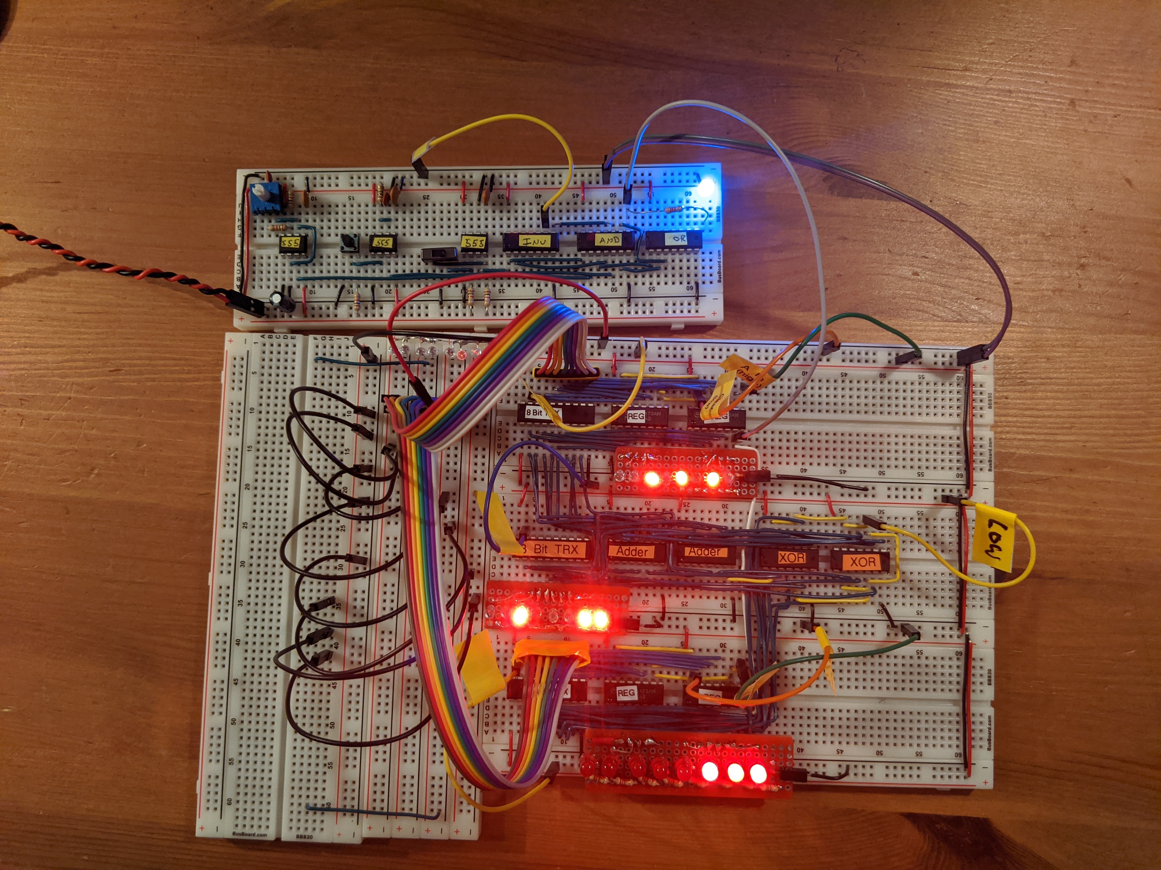
The ALU
The ALU reads directly from the A and B registers and computes the sum of those two values. It bypasses the bus and reads directly from the registers, whether or not they are set to output their values. The ALU has two modes, add and subtract.
In subtract mode (when the control line is brought high), it subtracts the value in register B from register A. Subtraction works by negating the output of the B register and then adding that negative number to A. Two’s Complement is used to represent a negative number in binary. This pretty much boils down to flipping all the bit and then adding one. Eight XOR gates are used to flip the bits (the subtract signal is the other input to the gate) and then add one by setting the carry bit on the adder high. The carry bit is normally used when using multiple 4-bit adder chips together to add 8 bits together (or 12 or 16… etc).
Building and Debugging
So far this is has been the most complicated part of the computer to build. This is purely because of the number of connections to be made and how much they overlap. If you’re off by one pin for one wire the entire output is messed up and you have to wade through all the criss crossing wires to figure out what is wrong. The problem gets worse when you have multiple wires in the wrong spot… which is what happened to me.
I learned two useful approaches to this problem
- Write out a table of all of the connections
- Use a multimeter to test for voltage levels in addition to continuity
Tabling Connections
In order to know which if a wire is connecting the wrong pins on two IC’s, you need to know which are the right pins. So after blindly staring at the forest of wires, I went back to the pin outs of the IC’s and wrote a few tables to track what I should expect to be where. I did them by hand in a notebook, but this is essentially what I have.
The A Input
The A register is simpler than the B register since it connects directly to the adder and does not need to be negated.
| A Register Bit | A Transceiver Pin | Adder Pin Name | Adder Pin |
|---|---|---|---|
| 8 | 2 | A4 | Left 12 |
| 7 | 3 | A3 | Left 14 |
| 6 | 4 | A2 | Left 3 |
| 5 | 5 | A1 | Left 5 |
| 4 | 6 | A4 | Right 12 |
| 3 | 7 | A3 | Right 14 |
| 2 | 8 | A2 | Right 3 |
| 1 | 9 | A1 | Right 5 |
This basically just tells me that if I think I’m having an issue with the most significant bit in the A register (bit 8), then I need to check to see if the wire from the transceiver’s second pin connects to the twelfth pin on the left adder. Once I run down all the pins combinations to make sure that they are correct, I can be confident that the register is wired up correctly and move on to the B register.
The B Input
As alluded to above, the B register is a touch more complicated because it goes through a set of XOR IC’s as well.
| B Register Bit | B Transceiver Pin | XOR Pin Name | XOR Pin |
|---|---|---|---|
| 8 | 2 | A4 | Left 12 |
| 7 | 3 | A3 | Left 9 |
| 6 | 4 | A2 | Left 4 |
| 5 | 5 | A1 | Left 1 |
| 4 | 6 | A4 | Right 12 |
| 3 | 7 | A3 | Right 9 |
| 2 | 8 | A2 | Right 4 |
| 1 | 9 | A1 | Right 1 |
The other input pins on the XOR chips were easy and didn’t really require a complex table. All of the B pins were connected to eachother and then the carry in bit on the rigth adder
| Pin Name | XOR Pin |
|---|---|
| XOR B4 | Left 14 |
| XOR B3 | Left 10 |
| XOR B2 | Left 5 |
| XOR B1 | Left 2 |
| XOR B4 | Right 14 |
| XOR B3 | Right 10 |
| XOR B2 | Right 5 |
| XOR B1 | Right 2 |
| Adder Carry In | 7 |
And then the output of the XOR chips feeds back into the two adders
| B Register Bit | XOR Pin Name | XOR Pin | Adder Pin Name | Adder Pin |
|---|---|---|---|---|
| 8 | Y4 | Left 11 | B4 | Left 11 |
| 7 | Y3 | Left 8 | B3 | Left 15 |
| 6 | Y2 | Left 6 | B2 | Left 2 |
| 5 | Y1 | Left 2 | B1 | Left 6 |
| 4 | Y4 | Right 11 | B4 | Right 11 |
| 3 | Y3 | Right 8 | B3 | Right 15 |
| 2 | Y2 | Right 6 | B2 | Right 2 |
| 1 | Y1 | Right 2 | B1 | Right 6 |
One of the bigger mistakes here is that I wired the left XOR to the right adder. Not sure why I was so certain that was the right thing to do at the time but I did it consciously and certain that it would work out.
Adder Output
And now all that we need to do is wire the adder outputs to the transceiver.
| Summation Bit | Output Transceiver Pin | Adder Pin Name | Adder Pin |
|---|---|---|---|
| 8 | 2 | Left Σ4 | Left 11 |
| 7 | 3 | Left Σ3 | Left 15 |
| 6 | 4 | Left Σ2 | Left 2 |
| 5 | 5 | Left Σ1 | Left 6 |
| 4 | 6 | Right Σ4 | Right 11 |
| 3 | 7 | Right Σ3 | Right 15 |
| 2 | 8 | Right Σ2 | Right 2 |
| 1 | 9 | Right Σ1 | Right 6 |
Using a Multimeter
The most straightforward way to use the multimeter to verify the connections is to use the continuity feature:
- Turn on the multimeter
- Put the red lead on one pin
- Put the black lead on the pin you hope it’s connected to (this is where the charts come in handy)
If you hear a tone, then the wiring is good. If you don’t, then you found a problem. Move the black lead to other pins to determine which pin the other end of the wire is connected to. Even if there was a tone, it may be useful to place the black lead on other pins to check for a short. This would mean that another wire connected to this IC is incorrect.
The upside of this approach is that it is simple. The downside is that it requires testing every connection. This is a pretty simple layout and it has upwards of forty connections to check. Another option is to do voltage reading to test which connections have voltage running through them. This is essentially the same as hooking up an LED in parallel to each of the pins to see its output. Set the multimeter to 5v DC setting, put the black wire to ground, and then put the red wire on the IC pin. I like to use alligator clamps coming out of the multimeter connected to jumper wires. That way the wires can be plugged directly into the breadboard and you can monitor voltages as the state changes.
Output
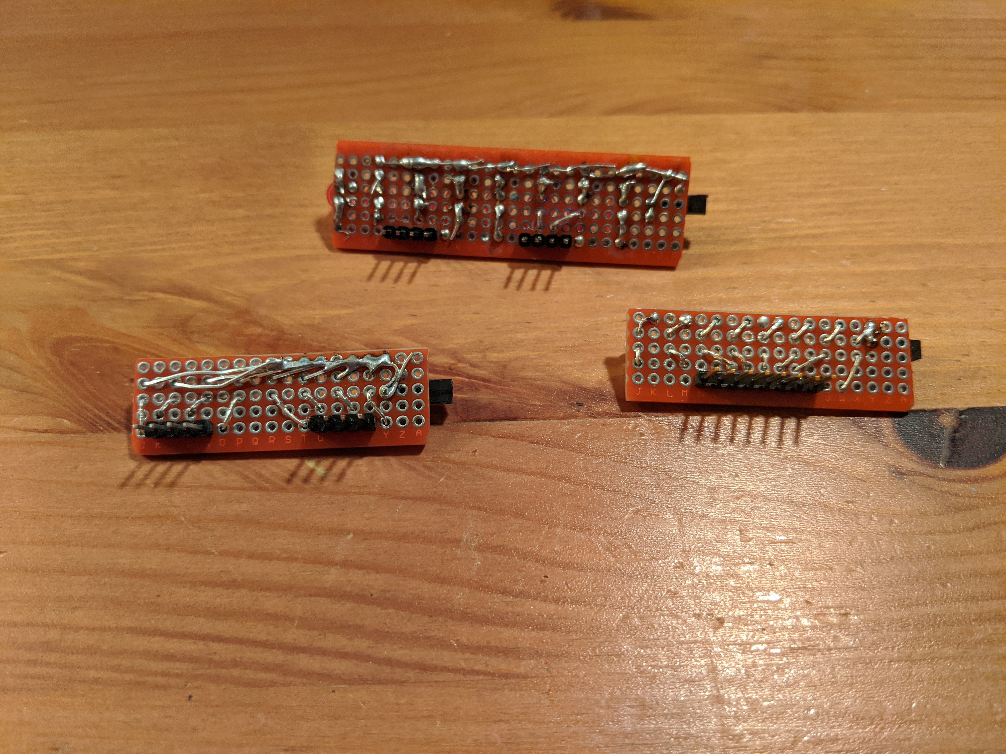
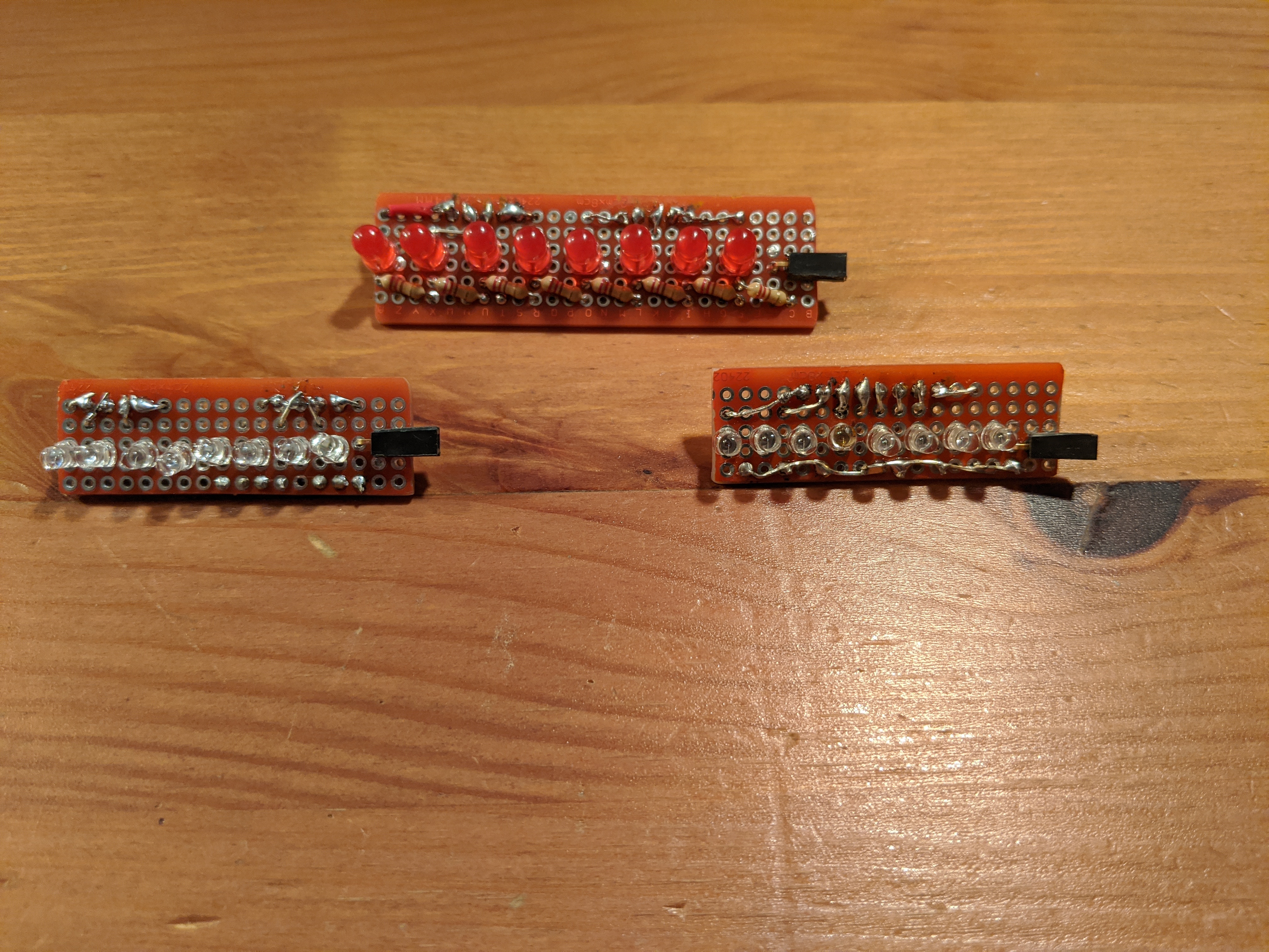
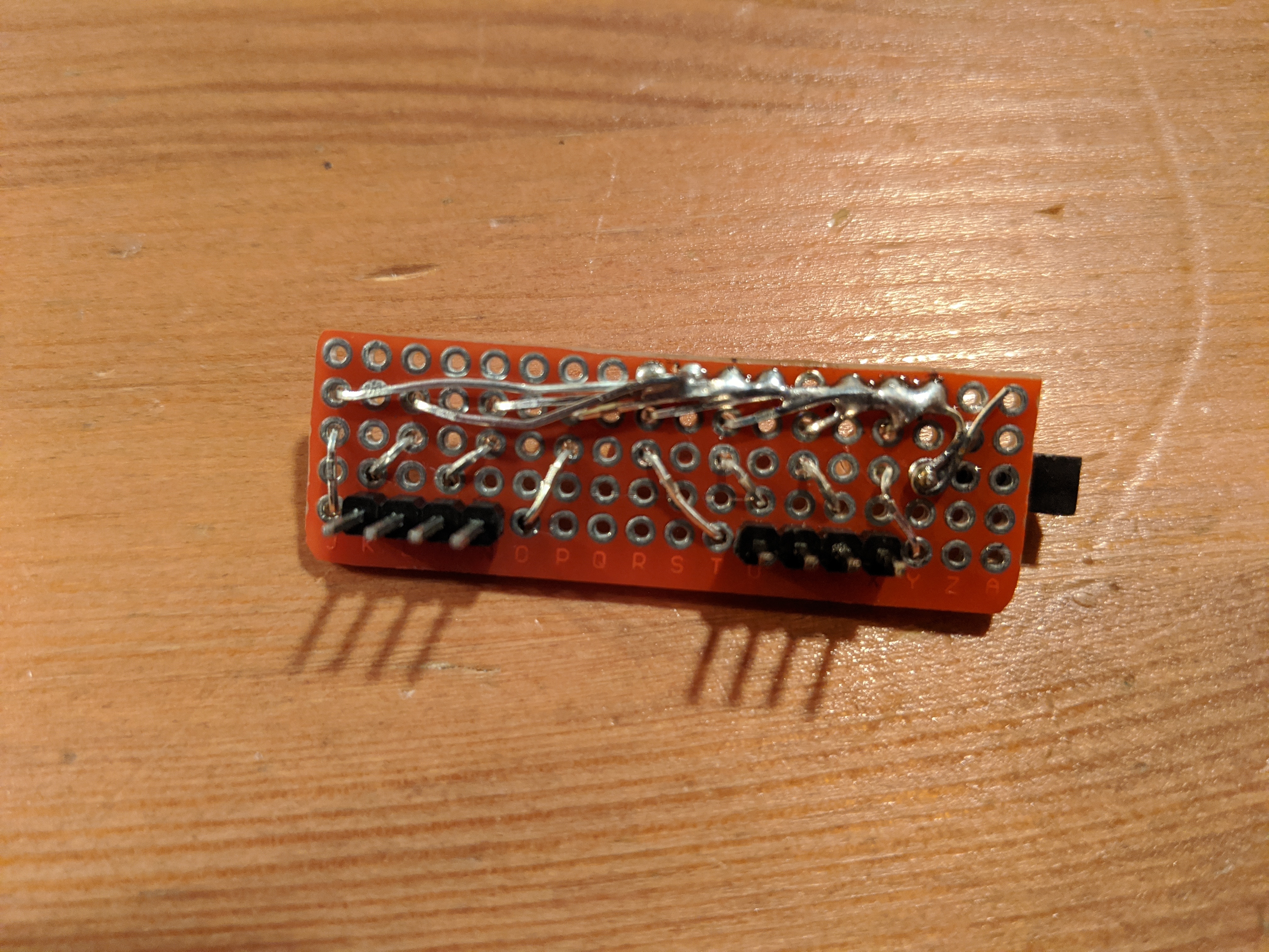
The final component here is wiring up LED’s. I decided it would be easiest to read the output if I made more LED strips that could plug into the breadboard with headers. I’ve improved on the original design by using LED’s with with the resistors built in. This reduces the amount of soldering I need to do and makes the result a little more compact. Speaking of which, I also used 3mm LED’s instead of the original 5mm.